Facilities
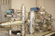
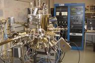
Semiconductor and Nanostructures Epitaxy:


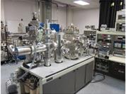
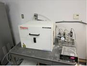
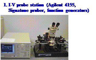
Materials/Devices Characterization and Processing:
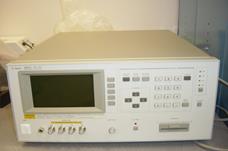
2. LCR Meter (Agilent 4284A)
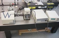
4. Photoluminescence and Electroluminescence 3. Photocurrent Spectroscopy
6. Hybond
572A Wedge wire bonder
Other materials and devices
characterization capability available in UCR:
1)
Analytical Microscopy User
Facility, including SEM and TEM
2)
UCR Optical User
Facility, including XRD, FTIR, Raman Spectroscopy, Scanning UV/VIS/IR
Spectrophotometer, etc.
Device Fabrication:
2. UCLA Nanofabrication User
Facility
3. Stanford Nanofabrication Facility